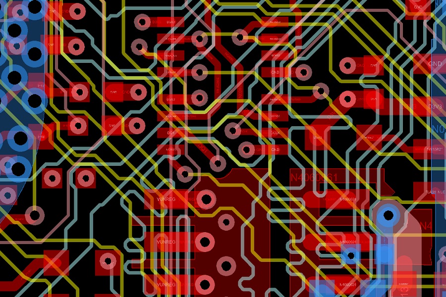
PCB layout
Stadigt voksende bus data hastigheder fører til stadigt voksende kompleksitet i PCB’et.
Det er i dag obligatorisk at udføre en række forskellige analyser for at sikre, at PCB’et fungerer korrekt:
Opretholdelse af konstant impedans af net, der spænder over flere formfaktorer, stort transmissionstab forårsaget af laminatmaterialer, højt termisk effekttab og temperatur-stigningger i komponenter og kobber.
For ikke at glemme de fejl-tests der skal laves for at sikre, at produktet lever op til specifikationerne.